

Description
From Design to Silicon brings together industry leaders and technical experts to share perspectives on how semiconductor products are conceived, designed, verified, implemented, manufactured and brought to market. The workshop will explore the engineering challenges, technology shifts and design methodologies shaping the semiconductor industry, from digital design, verification and physical implementation to high-speed interfaces, EDA innovation, advanced semiconductor technologies and emerging AI-enabled workflows. Participants will gain direct insight into how experienced engineers approach complex design challenges, make critical decisions, navigate trade-offs and translate technical innovation into successful silicon.
Developed with input from Canadian semiconductor employers and the Industry Training Advisory Group (ITAG).
Agenda
| Time (PM ET) | Presenter | Organization | Title |
|---|---|---|---|
| 1:00–1:10 | Yassine Hariri | CMC Microsystems | Welcome and opening remarks |
| 1:10–1:35 | Serge Patenaude | Fidus Systems | A Bug’s Life: Three Decades in the ASIC/FPGA Trenches |
| 1:35–2:00 | Dustin Dunwell | Qualcomm | Wasting Millions: How Simple Mistakes Can Ruin Your Sleep and Bankrupt Your Company |
| 2:00–2:25 | Francis Beaudoin | Cadence | Circuit Meets Reality: High-Speed Mixed-Signal Challenges from Design to Production |
| 2:25–2:35 | Break | ||
| 2:35–3:00 | Olivier Robert | Cadence | Beyond the Ideal Flow: Agility in Real-World Physical Design |
| 3:00–3:25 | Bob Tsai | Siemens EDA | TBD |
| 3:25–3:50 | Steve Kornachuk | TSMC | Introduction to TSMC & Enabling the AI Revolution |
| 3:50–4:25 | Industry Panel: The Realities of Getting to Silicon Moderator: Udson Mendes, CMC Microsystems | ||
| 4:25–4:30 | Yassine Hariri | CMC Microsystems | Closing remarks |
Target Attendees
Participants in the Semiconductor Upskilling Training Program, early-career engineers, professors, research associates, graduate students, and industry professionals interested in semiconductor design, verification, high-speed mixed-signal systems, foundry technologies, production, and AI.
What You Will Learn
- Connect semiconductor training to real industry practice
- Expose participants to engineering judgement, trade-offs and lessons learned
- Show how decisions across the design-to-silicon lifecycle affect product success
- Create direct interaction with experienced semiconductor industry experts
Topics Covered
- ASIC/FPGA engineering and verification
- Design mistakes, silicon re-spins and business impact
- High-speed mixed-signal design from design to production
- Physical design and implementation
- Foundry technologies, advanced semiconductor processes and AI
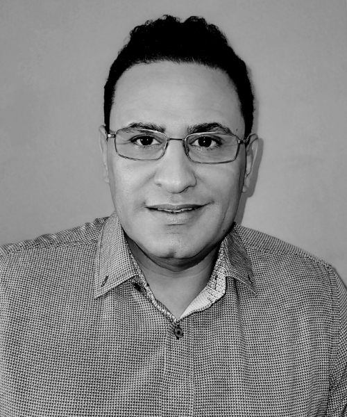
Yassine Hariri
CMC Microsystems
Yassine has over 17 years of experience developing and deploying advanced technologies at the intersection of IoT, edge AI, semiconductor design, and cloud-to-edge computing. He currently leads a national semiconductor upskilling initiative designed to strengthen Canada’s talent pipeline and bridge the gap between academic preparation and industry contribution.
His work connects workforce development, semiconductor infrastructure, industry engagement, and practical training pathways that support Canada’s capacity in strategic sectors such as clean technology, advanced manufacturing, health, space, and defence. At CMC Microsystems, he has contributed to national microsystems and semiconductor initiatives, supported major infrastructure and ecosystem programs, and led technology platforms that help Canadian researchers, startups, manufacturers, and industry partners translate advanced research into practical, reusable, and deployable solutions. He received the B.S. degree in Electrical Engineering from École Marocaine des Sciences de l’Ingénieur, Casablanca, Morocco, in 1998, and the M.S. and Ph.D. degrees in Electrical Engineering from École de technologie supérieure, Montréal, QC, Canada, in 2002 and 2008, respectively.
Serge Patenaude
Fidus Systems
Veteran ASIC/FPGA Verification Consultant/Architect with nearly 30 years of experience. Deep knowledge of the industry, built-up from background in the telecommunication, wireless (including voice, data and video), graphic cards and aerospace industries.
Fully aware of product life cycle challenges and time to market real-life constraints. Project size scaling from tiny gate arrays to multi-billion transistor monsters. Career balanced between high-stakes service consulting—delivering rapid solutions for critical client crises—and working within product giants to architect long-term verification strategies. Three decades of adapting to evolving tools, languages, and methodologies, resulting in a comprehensive, 360-degree view of how to successfully validate complex silicon. Experience in machine learning and deep learning using Python (Tensor Flow, SciKit-Learn).
Dustin Dunwell
Qualcomm
Dustin Dunwell is a Senior Director at Qualcomm Technologies, where he leads teams developing advanced semiconductor and wireline technologies. He holds a PhD in Electronics from the University of Toronto and has built his career at the intersection of engineering, technology innovation, and leadership.
Dustin is also an active IEEE volunteer leader and has held leadership roles within IEEE Toronto Section, IEEE Canada, and the IEEE Solid-State Circuits Society. He is the organizer of the IEEE Canada Students and Young Professionals (CSYP) Congress, bringing together emerging engineering talent, industry leaders, and IEEE volunteers from across Canada. Through both his professional and IEEE leadership, Dustin is passionate about advancing technology, developing the next generation of engineering leaders, and strengthening connections between industry, academia, and the broader engineering community.
Francis Beaudoin
Cadence
Francis Beaudoin is a Design Engineering Architect at Cadence with over two decades of technical leadership and design expertise in SerDes semiconductors. Based in Montreal, Canada, he holds a Master of Engineering degree from McGill University.
He has contributed to the architecture and development of high-speed IC and SerDes technologies at Alphawave Semi, Microchip Technology, and PMC-Sierra, with expertise spanning DFE-based NRZ receivers, SAR ADC-based PAM4 receiver architectures, RFIC design, and multi-generation wireline communication systems, while also leading system-level product and architecture development initiatives at Current (powered by GE) and Keurig Canada. His experience spans the full semiconductor development lifecycle, from architecture and design to silicon validation and production bring-up, enabling him to bridge rigorous engineering principles with practical industry execution.
Olivier Robert
Cadence Design Systems
Olivier is a Sr Principal Engineering Designer at Cadence Design Systems in Montreal. With over 15 years of experience in the semiconductor industry, he currently serves as a Physical Design IP Lead involved in all implementation aspects and methodology development for digital back-end flows.
His technical expertise encompasses the complete physical design cycle as well as analog macros integration. He has extensive advanced-node experience across TSMC (down to A14), Intel, GF, and Samsung foundries. Backed by a track record of multiple successful tape-outs, he has a strong interest in analog macro characterization for digital integration, as well as leveraging Language Models (LLMs) to achieve shorter turnaround times during physical implementation.
Steve Kornachuk
TSMC
Steve is a veteran semiconductor IP designer with experience building low power and high-performance silicon for networking, server CPU, mobile, and AI applications.
After graduating from the University of Ottawa, Steve began his career at Bell-Northern Research and Nortel, specializing in Content Addressable Memory (CAM), low-power SRAM, and high-performance SRAM. Over his career he has led design teams at startups as well as industry leaders like Intel, Apple, and TSMC, with development mandates ranging from embedded custom and compiled circuit IP to full SoC products.
Bob Tsai
Siemens
Bob’s team in Saskatoon, SK, Canada focuses on ramping up fresh grad talents into experienced Application Engineers to drive the adoption and deployment of Aprisa, Siemens EDA’ digital implementation solution.
Udson Mendes
CMC Microsystems
Udson is Director of Technology at CMC Microsystems, where he leads a team of 17 professionals supporting the FABrIC program across quantum technologies, photonics, microelectronics, MEMS, and IoT/Edge AI.
He is responsible for developing and scaling technology initiatives that bridge advanced research and commercial impact, helping strengthen Canada’s deep-tech innovation ecosystem.
Among his recent accomplishments, Udson conceived and launched Canada’s first Quantum Computing Sandbox and led the development of the Semiconductor Upskilling Training Program from concept to implementation. Over the past five years, he has secured more than CAD $1.15 million in grants and industry sponsorships to support technology training and workforce development initiatives.
Udson’s technical expertise is rooted in superconducting and silicon-based quantum hardware research. He is the author of peer-reviewed publications in leading scientific journals, including Nature, Science, and Nature Communications. He holds a PhD in Physics and has completed the Mini-MBA program at McGill University. In 2025, he was awarded the Medalha de Honra UFG by the Universidade Federal de Goiás, a distinction presented every four years to 30 alumni in recognition of their contributions to society.